ASML
PAS 5500 300 C

Wafer size
Wafer Alignment:
Performance
ATHENA+TIS 3X0 (Off Axis Alignment System)[1]
Optics
Resolution <0.25um[1]
What it is
The ASML PAS 5500 / 300 C is a deep-ultraviolet (DUV) wafer stepper used in semiconductor photolithography. The machine is a step-and-repeat projection system that exposes a reticle pattern onto a wafer one field at a time. The PAS 5500/300C is capable of processing 88 200-mm wafers per hour. The system belongs to ASML's PAS 5500 family of lithography tools.[1][2]
The PAS 5500/300C is a DUV stepper that operates at a wavelength of 248 nm. The system uses a Cymer ELS 5610 excimer laser as its illumination source. The stepper incorporates an AERIAL Illuminator, which allows extendibility beyond 0.25 µm without compromising the excellent imaging performance and high productivity.[1][2]
How it works
The PAS 5500/300C is a projection printer that uses a DUV (248 nm) lens column (0.63 N.A.) to provide a 4:1 reduction with an exposure field size up to 22 mm square. Minimum feature size is <0.20µm. The number and placement of the dies is programmable. Wafer sizes of 3" up to 200 mm can be accommodated, and pieces with significant effort. Registered alignment is typically <0.045µm, even when using backside alignment. 6" x 0.250"-thick quartz masks are used.[3]
The wafer stage is an air-bearing exposure stage with a SiSiC wafer table (200 mm) that can be set up to run 125–200 mm wafers. The reticle alignment is TTL dual-beam alignment. The wafer alignment system uses ATHENA+TIS 3X0 off-axis alignment that supports PM, XPA, SPM and NSSM marks. The system has an image sensor (IQC) for fast automated verification of focus and overlay. The leveling and autofocus system uses two measurement systems: a coarse red measurement system (820 nm) with a capture range of +/- 400 µm, and a fine white measurement system (725–1050 nm) with a capture range of +/- 23 µm. Three measurement methods are available: global leveling (3 points on a wafer, red), coarse leveling (1 point levels the die before exposure, red), and fine leveling (4 or fewer points in the exposure slit, white).[1]
Where it fits in the process flow
The PAS 5500/300C is capable of processing 88 200 mm wafers per hour. The system supports 8-inch (200 mm) wafers as its primary wafer size, but can also handle 125 mm and 150 mm wafers. The stepper is designed for high-volume production of semiconductor devices at the 0.25 µm technology node and beyond.[1][2]
Applications
The stepper can be used to pattern a variety of substrates, including silicon, gallium arsenide (GaAs), and indium phosphide (InP). The system supports the use of standard SEMI-spec wafers with carrier wafers approved by photolithography staff. The back of the substrate must be clean (no resist), and the mask must be clean (no resist or fingerprints).[3]
Why won't it start?
Documented failure modes, common issues, and field considerations.
- Ceased numerical aperture motor at 0.57
- Lens was still usable at 79% of production
What do the numbers mean?
Wafer handling9
- Wafer Stage Type
- Air Bearing Exposure Stage 200mm, SiSiC Wafer Table (Can be set up to run 125-200mm wafers)[1]
Optics & imaging14
- Resolution <0.25um[1]
- uDOF >0.7 um at 0.25um and distortion <35nm with Conventional Illumination[1]
- Illumination:[1]
- AERIAL Illumination System[1]
- Zoom Annual Illumination[1]
- 4 Independent Full Field Reticle Masking[1]
- Levelling/autofocus
- Two measurement systems: coarse red measurement system (820 nm) and fine white measurement system (725-1050 nm)[1]
Performance2
- ATHENA+TIS 3X0 (Off Axis Alignment System)[1]
Control & software2
Configuration & options11
Vintage & configurations
Documented models & variants
| Designation | Generation | Vintage | Changes | Source |
|---|---|---|---|---|
| PAS 5500/300C | DUV | — | Capable of processing 88 200 mm wafers per hour and incorporates an AERIAL Illuminator. | web.archive.org[2] |
Where are the manuals?
Publicly hosted documents referencing this tool, linked at their original location. Hosted by the linked institutions — availability may change.
- DUV Resist InformationDocumentcornell.edu
Generated from public-source data on file. Enter your email to access — nothing is published; details are routed privately.
Not publicly documented
Field notes
No research found yet — worked with this tool? Share what you know.
Frequently asked questions
What is the exposure wavelength of the ASML PAS 5500/300C?
The ASML PAS 5500/300C uses a 248 nm DUV exposure wavelength from a Cymer ELS 5610 excimer laser.[1]
What wafer sizes does the PAS 5500/300C support?
The PAS 5500/300C supports 125, 150, and 200 mm wafers (3" up to 200 mm with pieces). The system is configured for 200 mm (8-inch) wafers as its primary size.[1][3]
What is the maximum throughput of the PAS 5500/300C?
The PAS 5500/300C is capable of processing 88 200 mm wafers per hour.[2]
Not publicly documented
The following facts about the PAS 5500 300 C are absent from this record as of this revision. First-hand knowledge or a citation closes a gap; every submission is reviewed before publication.
No publicly documented production dates or lifecycle milestones (introduction, end of production, EOL) for the PAS 5500 300 C are on record.
Answerable by: OEM historical records or a trade-press announcement
The control-system platform and OS era of the PAS 5500 300 C are not on record.
Answerable by: an engineer who operated it or OEM installation records
The process node or technology generation of the PAS 5500 300 C is not on record.
Answerable by: an OEM datasheet or a fab qualification report
No publicly documented compatible parts, consumables, or accessories for the PAS 5500 300 C are on record.
Answerable by: an OEM parts catalog or a service engineer
Sources & citations
Sources (4)Every fact above is drawn from these public sources
- [1]Inventory photo
- [2]web.archive.org — asml.com (Jan 25, 2006)web.archive.org
- [3]ASML PAS 5500/300C DUV Wafer Stepper | CNF Users — cnfusers.cornell.educnfusers.cornell.edu
- [4]Equipment Resources | CNF — cnf.cornell.educnf.cornell.edu
Last updated Sep 22, 2026.
Compare with similar tools
View all →Brooks 017-0146-01 is a prealigner manufactured by Brooks.
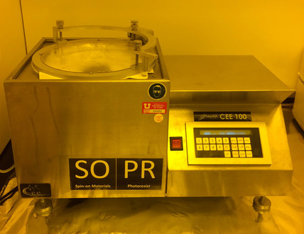
The CEE 100 is a lithography spin coater/developer tool that accepts up to 6-inch wafers and supports programmable multi-step processing.